
 EN


I2C IO Expander Design Guide: 16-Bit Bidirectional GPIO Expansion and 1.65V–5.5V Level Translation with the ETEK ET6416
 2026/11/16
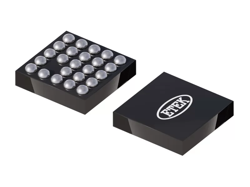
An I2C IO expander is a serial-to-parallel interface IC that enables a host microcontroller (MCU), microprocessor, or FPGA to control and monitor up to 16 additional general-purpose input/output (GPIO) pins using only two wires—serial clock (SCL) and serial data (SDA). By offloading low-speed control signals, keypad matrices, fault inputs, and LED indicators onto a shared two-wire bus, engineers can select smaller, lower-cost host processors and dramatically reduce board-to-board connector pin counts.
To eliminate the need for separate voltage translators in mixed-supply systems, ETEK Microelectronics designed the ET6416, a 16-bit I²C-bus and SMBus I/O expander featuring independent dual supply rails (VDDI and VDDP, both operating from 1.65V to 5.5V) for built-in bidirectional voltage-level translation, 400 kHz Fast-mode I²C operation, an open-drain interrupt output (INT), an active-low hardware reset (RESET), 25 mA LED sink capability, and ultra-low 1.0 µA typical standby current (at 3.3V) in ultra-compact VFBGA24 (3 mm × 3 mm) and QFN24 (4 mm × 4 mm) packages.
In this technical design guide, you will learn:
- How a dual-supply 16-bit I2C IO expander simultaneously solves GPIO pin shortages and mixed-voltage translation
- How to configure the ET6416’s four register pairs (00h–07h) for input sensing, output driving, and polarity inversion
- How event-driven interrupt signaling (INT) eliminates continuous I²C bus polling
- Pinout comparisons (VFBGA24 vs. QFN24), slave addressing (0x20 / 0x21), and PCB design best practices
What Is an I2C IO Expander and Why Dual-Supply Architecture Matters?
An I2C IO expander acts as a remote register-mapped GPIO bank on the I²C or SMBus serial interface. Every port pin (P0_0–P0_7 on Port 0 and P1_0–P1_7 on Port 1) can be independently programmed as a high-impedance digital input or a push-pull CMOS output via software register writes.
In conventional single-supply I/O expanders, the SCL/SDA serial interface and the 16 parallel GPIO pins share a single VDD pin. When a modern 1.8V core SoC needs to monitor 3.3V or 5.0V industrial sensors, DIP switches, or power-good flags, engineers are forced to add an external bidirectional level shifter on the I²C bus.
The ET6416 solves this at the silicon level by splitting its power architecture into two independent supply domains:
- VDDI (1.65V to 5.5V): Powers the I²C-bus interface (SCL, SDA, and RESET), connecting directly to the host microcontroller’s I/O voltage rail (1.8V, 2.5V, 3.3V, or 5.0V).
- VDDP (1.65V to 5.5V): Powers the core logic, ADDR pin, and the 16 parallel peripheral ports (P0_0–P0_7 and P1_0–P1_7), operating at any peripheral voltage rail (1.8V, 2.5V, 3.3V, or 5.0V).
Three System Design Bottlenecks Solved by the ET6416
1. Eliminating External Level Shifters Across Mixed Voltage Domains
As specified in the ET6416 Datasheet (Rev 1.6), the dual-rail design provides seamless bidirectional level translation across all standard logic nodes without external components:
| Host I²C Bus Voltage (VDDI on SCL/SDA) | Supported Port P Voltage (VDDP on P0_0–P1_7) | Typical Mixed-Signal Application Scenario |
|---|---|---|
| 1.8V SCL/SDA | 1.8V, 2.5V, 3.3V, or 5.0V Port P | 1.8V application processor controlling 3.3V/5V relays, LEDs, and board sensors |
| 2.5V SCL/SDA | 1.8V, 2.5V, 3.3V, or 5.0V Port P | 2.5V FPGA I/O bank managing multi-rail power-supply enable and PG signals |
| 3.3V SCL/SDA | 1.8V, 2.5V, 3.3V, or 5.0V Port P | 3.3V industrial MCU interfacing with 1.8V low-power sensors or 5V legacy logic |
| 5.0V SCL/SDA | 1.8V, 2.5V, 3.3V, or 5.0V Port P | 5.0V automotive/appliance controller expanding 1.8V/3.3V sub-module GPIOs |
2. Event-Driven Interrupts (INT) Instead of Wasteful Bus Polling
Polling 16 remote inputs continuously over a 400 kHz I²C bus wastes MCU instruction cycles, increases bus traffic, and prevents battery-powered hosts from entering deep sleep. The ET6416 integrates an open-drain, active-LOW interrupt output (INT) that asserts within 1 µs max (tvINT) whenever any pin configured as an input changes state (on either a rising or falling edge) relative to the stored Input Port register value.
Instead of polling over I²C, the host MCU monitors a single interrupt line and only reads the ET6416 when an actual keypad press, alarm signal, or card-detect event occurs. Reading the port register that triggered the event (or the input returning to its original state) automatically clears the INT flag on the ACK/NACK clock pulse.
3. Direct 25 mA LED Sink Drive and Glitch-Free Power-Up
Driving status LEDs on server front panels, telecom blades, or industrial HMIs typically requires external transistor arrays. Each Port P output on the ET6416 supports up to 25 mA sink current (recommended continuous IOL ≤ 23 mA per pin, IOH ≤ 10 mA source, total Port P supply current IDDP ≤ 160 mA), allowing direct connection to indicator LEDs. On power-up, an internal Power-On Reset (VPOR = 1.1V typical) initializes all 16 ports as glitch-free high-impedance inputs, preventing accidental relay actuation or LED flashes during system boot.
Inside the ET6416 Register Architecture and I2C Protocol
Hardware Slave Addressing (0x20 and 0x21)
The ET6416 uses a 7-bit I²C slave address formatted as 0100 00[ADDR] followed by the R/W bit (0 for write, 1 for read), where the ADDR pin is tied directly to GND (VSS) or VDDP:
- ADDR = GND (Logic 0): 7-bit Slave Address = 0x20 (0100 000b → 0x40 Write / 0x41 Read)
- ADDR = VDDP (Logic 1): 7-bit Slave Address = 0x21 (0100 001b → 0x42 Write / 0x43 Read)
This allows two ET6416 devices to share the same I²C bus without an I²C multiplexer, providing 32 expanded GPIOs over two wires.
Complete 8-Register Map (00h to 07h)
Following the slave address byte, the host master writes a Command Byte to the internal Pointer Register (00h–07h). The eight 8-bit registers are organized as four register pairs (Port 0 and Port 1); writing or reading sequentially automatically toggles between the two registers in the selected pair:
| Command Byte | Register Name | Target Port Pins | Read/Write Access | Power-Up Default | Functional Behavior |
|---|---|---|---|---|---|
| 00h | Input Port 0 | I0.7–I0.0 (P0_7–P0_0) | Read-Only | XXXX XXXXb | Reflects live logic level on Port 0 pins (whether configured as input or output) |
| 01h | Input Port 1 | I1.7–I1.0 (P1_7–P1_0) | Read-Only | XXXX XXXXb | Reflects live logic level on Port 1 pins (whether configured as input or output) |
| 02h | Output Port 0 | O0.7–O0.0 (P0_7–P0_0) | Read / Write | 1111 1111b (FFh) | Sets output latch state for Port 0 pins enabled as outputs (0 = LOW, 1 = HIGH) |
| 03h | Output Port 1 | O1.7–O1.0 (P1_7–P1_0) | Read / Write | 1111 1111b (FFh) | Sets output latch state for Port 1 pins enabled as outputs (0 = LOW, 1 = HIGH) |
| 04h | Polarity Inversion 0 | N0.7–N0.0 (P0_7–P0_0) | Read / Write | 0000 0000b (00h) | Inverts read value in Input Port 0 when bit = 1; retains normal polarity when bit = 0 |
| 05h | Polarity Inversion 1 | N1.7–N1.0 (P1_7–P1_0) | Read / Write | 0000 0000b (00h) | Inverts read value in Input Port 1 when bit = 1; retains normal polarity when bit = 0 |
| 06h | Configuration 0 | C0.7–C0.0 (P0_7–P0_0) | Read / Write | 1111 1111b (FFh) | Configures Port 0 pin direction: 1 = High-impedance Input (default), 0 = Output |
| 07h | Configuration 1 | C1.7–C1.0 (P1_7–P1_0) | Read / Write | 1111 1111b (FFh) | Configures Port 1 pin direction: 1 = High-impedance Input (default), 0 = Output |
ET6416 Key Electrical and Timing Specifications (TA = -40°C to +85°C)
All values below are verified against the ET6416 Datasheet (Rev 1.6):
| Parameter | Symbol | Test Conditions | Min | Typ | Max | Unit |
|---|---|---|---|---|---|---|
| I²C-Bus Supply Voltage | VDDI | Independent host interface supply | 1.65 | — | 5.5 | V |
| Port P Supply Voltage | VDDP | Independent 16-bit I/O port supply | 1.65 | — | 5.5 | V |
| Standby Current (3.3V) | IDD | FSCL = 0 kHz, IO = 0 mA, inputs at rail (2.3V–3.6V) | — | 1.0 | 3.2 | µA |
| Standby Current (1.8V / 5.0V) | IDD | FSCL = 0 kHz @ 1.65V–2.3V / 3.6V–5.5V | — | 0.5 / 1.5 | 1.7 / 7.0 | µA |
| Operating Supply Current | IDD | FSCL = 400 kHz, IO = 0 mA (1.8V / 3.3V / 5.0V) | — | 4.0 / 6.5 / 10 | 9 / 15 / 25 | µA |
| Schmitt-Trigger Hysteresis | VHYS | SCL/SDA inputs @ 1.8V / 2.5V / 3.3V / 5.0V | — | 0.18 / 0.25 / 0.33 / 0.50 | — | V |
| Port P Sink Current (IOL) | IOL | VOL = 0.5V / 0.7V @ VDDP = 4.5V | 8 / 10 | 17 / 24 | 25 (max) | mA |
| Port P High Output (VOH) | VOH | IOH = -8 mA / -10 mA @ VDDP = 3.0V | 2.6 / 2.5 | — | — | V |
| I²C Clock Frequency | fSCL | Standard-Mode / Fast-Mode I²C | 0 | — | 100 / 400 | kHz |
| Input Spike Suppression | tSP | Pulse width filtered on SCL and SDA | 0 | — | 50 | ns |
| Port Output Valid Time | tvQ | From SCL edge to Port P output valid | — | — | 400 | ns |
| Interrupt Valid / Reset Time | tvINT / trstINT | Port P edge to INT valid / SCL to INT clear | — | — | 1.0 / 1.0 | µs |
| Hardware Reset Pulse / Time | tw(rst) / trst | Active-LOW pulse width on RESET / recovery | 30 | — | 600 | ns |
| ESD & Latch-Up Immunity | — | HBM / CDM / Latch-Up current | — | ±2000V / ±1000V / >100mA | — | — |
Package Comparison (ET6416 VFBGA24 vs. ET6416Y QFN24)
To support both ultra-dense portable modules and standard industrial SMT assembly, the ET6416 is offered in two 24-terminal packages:
| Ordering Part No. | Package Type | Body Dimensions | Pitch | Thermal Impedance (RθJA) | Key Pin / Ball Mapping (INT, VDDI, RESET, ADDR, SCL, SDA, VDDP, VSS) |
|---|---|---|---|---|---|
| ET6416 | VFBGA24 | 3.0 mm × 3.0 mm × 0.85 mm | 0.50 mm ball pitch | 171 °C/W | INT=A3, VDDI=B3, RESET=A2, ADDR=B5, SCL=A5, SDA=A4, VDDP=B4, VSS=E2 |
| ET6416Y | QFN24 | 4.0 mm × 4.0 mm × 0.75 mm | 0.50 mm lead pitch | — | INT=Pin 22, VDDI=Pin 23, RESET=Pin 24, ADDR=Pin 18, SCL=Pin 19, SDA=Pin 20, VDDP=Pin 21, VSS=Pin 9 |
Practical Hardware Design Guidelines for the ET6416
- Configure Unused or Suspended Port P Pins as Outputs: As noted in Section 10 and Figure 12 of the ET6416 Datasheet, never leave unused Port P pins floating in Input mode (Configuration bit = 1), because CMOS inputs floating near mid-supply (VDDP – 0.6V) draw additional shoot-through quiescent current (ΔIDD up to 80 µA) and can trigger false INT interrupts. Either write 0 to the corresponding Configuration Register bit to set unused pins as driven outputs, or tie them to VDDP/VSS via a pull-up/pull-down resistor.
- Pull Up SCL, SDA, RESET, and INT to the Correct Supply Rail:
- Pull SCL, SDA, and RESET up to VDDI (the host controller’s I²C supply voltage, e.g., 1.8V).
- Pull the open-drain INT pin up via a 10 kΩ resistor to the supply rail of the processor monitoring the interrupt (typically VDDI).
- Connect ADDR directly to either VDDP or VSS (GND)—do not connect ADDR to VDDI if VDDI > VDDP.
- Avoid False Interrupts When Switching Pin Direction: A pin configured as an output never generates an interrupt. However, dynamically reconfiguring a pin from output to input (0 → 1 in 06h/07h) can trigger an immediate interrupt if the external pin state differs from the previously latched value in Input Register 00h/01h. Read the Input Register immediately after changing direction to clear any transitional interrupt state.
- Recover Stuck I²C Buses via RESET Without Power Cycling: If a system noise glitch interrupts an I²C transaction mid-byte, asserting the active-LOW RESET pin for at least 30 ns (tw(rst)) resets the ET6416’s I²C/SMBus state machine and restores all registers to their power-on defaults within 600 ns (trst) while keeping VDDP powered.
Designing a complete mixed-voltage digital interface subsystem? Pair the ET6416 with our ETF0104 4-bit bidirectional level shifter for I2C, I3C, and SPI, our ETQ74LVC1G32 AEC-Q100 single 2-input OR gate, or our ET74HC4852 CMOS analog multiplexer. You can also browse ETEK’s full I/O Expander catalog and Signal Chain IC portfolio.
Frequently Asked Questions (FAQ)
How does the ET6416 I2C IO expander perform voltage level translation without an external level shifter?
The ET6416 features two separate supply pins: VDDI (1.65V–5.5V) for the SCL, SDA, and RESET host interface, and VDDP (1.65V–5.5V) for the 16 parallel I/O ports (P0_0–P0_7 and P1_0–P1_7). Internal level-shifting circuitry translates signals bidirectionally between VDDI and VDDP, allowing a 1.8V host MCU to directly read and drive 3.3V or 5.0V peripheral I/Os.
How many ET6416 I/O expanders can share a single I2C bus?
Two ET6416 devices can share the same I²C bus directly by tying the hardware ADDR pin to VSS (7-bit address 0x20) on the first chip and to VDDP (7-bit address 0x21) on the second chip, providing 32 expanded GPIO pins. If more than 32 GPIOs are required, multiple pairs can be placed behind an I²C bus switch or multiplexer.
Can the ET6416 directly drive LEDs without external buffer transistors?
Yes. Each Port P output pin can sink up to 25 mA maximum (24 mA typical at VDDP = 4.5V, VOL = 0.7V; 23 mA recommended continuous sink current), subject to the total Port P supply current limit (IDDP ≤ 160 mA and ground current IDD ≤ 200 mA). In addition, the built-in Polarity Inversion registers (04h and 05h) allow software to invert active-low switch inputs without external logic gates.
How should unused I/O pins on the ET6416 be terminated to minimize standby current?
At power-up, all 16 Port P pins default to high-impedance inputs (Configuration Registers 06h/07h = FFh). Any unused Port P pin should either be configured as an output (by writing 0 to its configuration bit) or tied to VDDP or VSS through an external resistor so the input buffer never floats near the switching threshold, preserving the ultra-low 1.0 µA typical standby current.
Conclusion: 16-Bit GPIO Expansion and Multi-Voltage Translation in One 3×3 mm IC
Whether you are expanding keypad, sensor, and alarm inputs in an industrial controller or driving status LEDs across 1.8V, 3.3V, and 5.0V rails in a server or telecom platform, the ET6416 combines a 400 kHz 16-bit I2C IO expander, dual-rail 1.65V–5.5V level translator, and 25 mA LED driver into a single VFBGA24 or QFN24 footprint.
👉 Visit the ET6416 product page, download the ET6416 datasheet, or explore ETEK’s I/O Expander IC lineup
✉️ Request Sample: https://www.etekmicro.com/sample


