
 EN


Logic Inverter Circuit: Working Principle and Applications
 2026/09/09
A logic inverter circuit is one of the fundamental building blocks of digital electronics. Its primary function is simple: it produces an output logic level opposite to the input. When the input is HIGH, the output becomes LOW; when the input is LOW, the output becomes HIGH. This basic Boolean operation is widely used in signal inversion, logic control, waveform processing, signal buffering, and digital interface circuits.
For engineers designing compact and low-power digital systems, the performance of the inverter itself can directly affect signal integrity, switching speed, power consumption, and system reliability. ETEK Microelectronics’ ET74LVC04A provides six independent inverter channels in a single device, combining wide-voltage operation, low power consumption, and strong output drive capability.
What Is a Logic Inverter Circuit?
A logic inverter circuit, also called a NOT gate, performs the Boolean function:
Y = NOT A
Its operation can be represented by a simple truth table:
| Input A | Output Y |
| HIGH | LOW |
| LOW | HIGH |
This means that the output always has the opposite logic state to the input. In practical digital systems, a logic inverter can be implemented using transistor-based logic gates or an integrated logic IC.
Beyond basic logic inversion, inverter devices can also be used to restore digital signal levels, drive downstream logic loads, and provide multiple independent inversion channels within a compact package.
How Does a Logic Inverter Circuit Work?
The core principle of a logic inverter circuit is to detect the input logic state and generate the complementary output state.
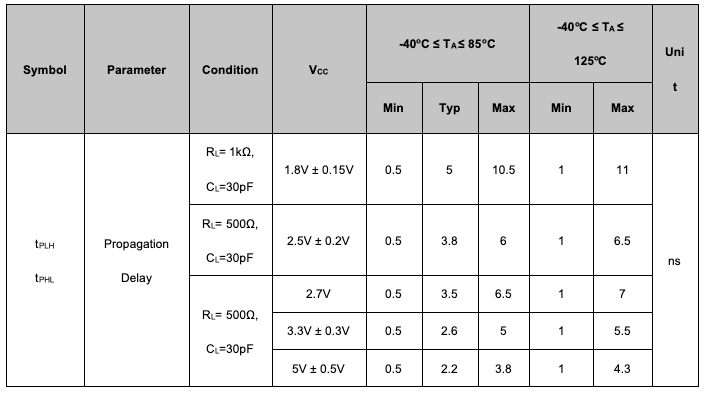
For example, when the input signal is LOW, the inverter switches its output HIGH. When the input changes to HIGH, the output switches LOW. The transition does not occur instantaneously; the time required for the output to respond to an input transition is known as propagation delay.
For the ET74LVC04A, the typical propagation delay at 5V is 2.2 ns under the specified test conditions, with a maximum of 3.8 ns over the -40°C to 85°C range.
This makes propagation delay an important parameter when selecting a logic inverter for high-speed digital signal applications.
ET74LVC04A: A Six-Channel Logic Inverter Solution
The ET74LVC04A integrates six independent inverters and operates from a 1.65V to 5.5V supply voltage, making it suitable for digital systems using different logic supply levels. Its inputs are also over-voltage tolerant up to 5.5V.
Key specifications include:
– Supply voltage: 1.65V to 5.5V
– Six independent inverter channels
– Quiescent supply current: 10µA max under the specified condition
– Input leakage current: ±1µA typical, ±20µA max
– Output sink/source capability: ±32mA
– Typical propagation delay: 8 ns at 5V as a general product feature; detailed AC testing specifies 2.2 ns typical at 5V under the datasheet test conditions
– Operating temperature: -40°C to +125°C
– ESD protection: ±4kV HBM and ±1kV CDM
– Packages: SOP14, TSSOP14, and DIP14
The device also supports outputs capable of driving up to 10 LSTTL loads, providing useful drive capability for digital control and signal distribution applications.
Why Choose a Wide-Voltage Logic Inverter?
Modern electronic systems frequently combine MCUs, sensors, interface ICs, and peripheral devices operating at different voltage levels. A logic inverter with a 1.65V–5.5V operating range gives designers greater flexibility when selecting the system supply voltage.
The ET74LVC04A can therefore be considered for applications requiring:
– Digital signal inversion
– Logic signal conditioning
– Control signal generation
– Signal buffering and distribution
– Microcontroller peripheral interfaces
– Consumer and industrial electronics
Its six independent channels can also reduce PCB component count when several inverted signals are required in the same circuit.
Package and Pin Configuration
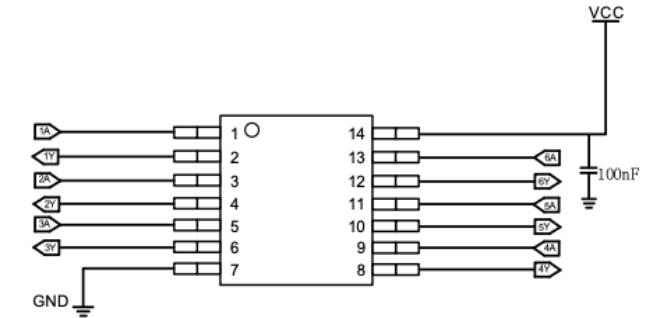
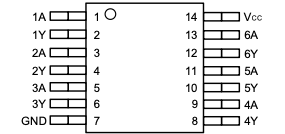
The ET74LVC04A is available in SOP14, TSSOP14, and DIP14 packages. Channels 1–3 are arranged on pins 1–6, while channels 4–6 occupy pins 8–13. Pin 7 is GND and pin 14 is VCC.
This standardized 14-pin configuration makes the device convenient for both new PCB designs and applications requiring multiple independent inverter gates.

Conclusion
A logic inverter circuit may perform a simple NOT operation, but its electrical characteristics are important in real-world digital systems. Supply-voltage range, propagation delay, output drive capability, leakage current, ESD protection, and package selection all influence the reliability and performance of the final design.
With six independent inverters, 1.65V–5.5V operation, ±32mA balanced output capability, low quiescent current, and multiple package options, the ET74LVC04A provides a flexible solution for a wide range of digital logic applications.
Learn more about the ET74LVC04A: ETEK ET74LVC04A Product Page
Request Sample: https://www.etekmicro.com/sample


