
 EN


CMOS LDO Regulator Design Guide: Combining 1.0 µA Quiescent Current with Fast Transient Response and Reverse Current Protection
 2026/10/26
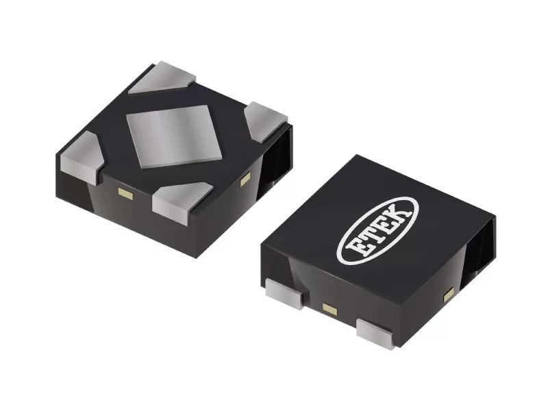
Selecting a CMOS LDO regulator for battery-powered wireless sensors, portable medical instruments, and smart utility meters requires balancing two historically opposing electrical metrics: ultra-low quiescent current (IQ) during standby and fast transient response during high-current radio transmission bursts. In duty-cycled Internet of Things (IoT) nodes that spend over 99% of their operational life in deep sleep, every microampere of continuous LDO ground current directly erodes multi-year battery runtime.
To eliminate this compromise, ETEK Microelectronics developed the ET63AXX series, a 300 mA ultra-low quiescent current CMOS LDO regulator featuring dynamic quiescent current control, integrated reverse current protection, and 70 dB power supply rejection ratio (PSRR).
In this article you will learn:
- What a CMOS LDO regulator is and why duty-cycled wireless loads challenge conventional designs
- How the ET63AXX achieves 1.0 µA quiescent current without sacrificing load-transient speed
- How integrated 20 mV reverse current protection eliminates external blocking diodes
- Package thermal limits and PCB layout rules for stable 1 µF ceramic capacitor operation
What Is a CMOS LDO Regulator?
A CMOS low-dropout (LDO) linear regulator uses a voltage-controlled PMOS pass transistor and a CMOS error amplifier to deliver a clean, regulated DC output voltage from a slightly higher input supply. Unlike legacy bipolar regulators whose base drive current rises with load current, a CMOS LDO regulator maintains microampere-level ground current across standby states while operating with a very small voltage differential (dropout voltage) between input and output.
Three Challenges in Low-Power IoT Voltage Regulation
1. The Quiescent Current vs. Transient Response Trade-Off
A fixed-bias 1 µA LDO has very limited current available to charge and discharge the gate capacitance of its internal PMOS pass FET. When a Bluetooth Low Energy (BLE), Zigbee, or Sub-GHz transceiver wakes up and pulls a fast current step from microamperes to hundreds of milliamperes, a slow control loop allows VOUT to droop below the MCU brownout threshold before the pass FET can open fully.
2. Reverse Body-Diode Conduction
Standard PMOS pass transistors contain an intrinsic parasitic body diode oriented from VOUT to VIN. If the input supply collapses, disconnects, or falls below the voltage held on output bulk capacitors or a backup cell, current flows backward from output to input—draining backup energy and potentially damaging the regulator.
3. Post-DC/DC Switching Ripple
When an LDO is used as a post-regulator after a buck or buck-boost converter to power RF synthesizers or precision analog sensors, poor power supply rejection allows switching noise to couple directly into the sensitive load.
How the ET63AXX CMOS LDO Regulator Solves Them
The ET63AXX is manufactured based on an advanced CMOS process and operates across an input voltage range from 1.7V to 5.5V, delivering up to 300 mA continuous output current across eight fixed output voltage options: 1.2V, 1.5V, 1.6V, 1.8V, 2.5V, 2.8V, 3.0V, and 3.3V with ±1.5% output voltage accuracy (IOUT = 1 mA, TA = 25°C).
Dynamic Quiescent Current Adjustment for Wireless Load Steps
Rather than relying on a static internal bias current, the ET63AXX incorporates a dynamic quiescent current circuit. Under no-load or microampere sleep conditions, the regulator consumes a typical quiescent current (IQ_ON) of just 1.0 µA (1.5 µA maximum at TA = 25°C), and drops to 0.01 µA typical (0.1 µA maximum) when disabled via the EN pin.
When the load current increases rapidly—such as during packet transmission in wireless communication modules—the dynamic bias circuit momentarily boosts internal loop bandwidth and gate-drive capability. This maintains tight load regulation (10 mV typical / 30 mV maximum for 1 mA ≤ IOUT ≤ 300 mA) and minimizes transient overshoot and undershoot without penalizing standby battery life.
True Reverse Current Protection (VOUT − VIN > 20 mV)
To eliminate external Schottky blocking diodes and their forward voltage drop, the ET63AXX integrates an active Reverse Current Protection comparator that monitors the differential voltage between the OUT and IN pins.
Whenever VOUT exceeds VIN by more than 20 mV (typical), the protection block switches both the gate and the substrate bulk of the internal PFET pass device to VOUT and turns the pass transistor completely off. As verified in the ET63AXX Datasheet, even under a severe reverse bias condition where VIN = 1.7V and VOUT = 5.5V, reverse leakage current (IRCB) is restricted to just 0.4 µA (typical). This makes the ET63AXX well suited for dual-supply OR-ing topologies, USB-plus-battery rails, and supercapacitor-backed metering circuits.
Low Dropout Voltage and Input-Following Behavior
Low dropout voltage (VDROP) extends usable battery capacity by allowing the regulator to maintain regulation as cell voltage decays toward end-of-discharge. At full 300 mA load (TA = 25°C), the ET63AXX achieves:
- VOUT = 3.3V: 210 mV (typical) / 400 mV (maximum)
- VOUT = 1.8V: 410 mV (typical) / 600 mV (maximum)
If the input voltage drops below the nominal regulated output level, the ET63AXX remains operationally stable and its output smoothly tracks the input voltage minus the resistive drop of the fully enhanced PMOS channel.
70 dB PSRR, Active Output Discharge, and Full Protection
Despite its 1.0 µA quiescent current budget, the ET63AXX achieves a power supply rejection ratio of 70 dB (typical) at 1 kHz (VIN = 2.8V, VOUT = 1.8V, COUT = 4.7 µF, IOUT = 20 mA) and an integrated output noise voltage (eN) of 120 µVRMS (typical) across the 10 Hz to 100 kHz bandwidth. Line regulation is held to 0.04 %/V (typical) (0.2 %/V maximum).
When the EN pin (ET63AXXYB and ET63AXX variants) is pulled below the logic-low threshold (VENL ≤ 0.4V), an internal N-channel discharge switch with a typical resistance (RLOW) of 110 Ω connects OUT to GND, rapidly discharging residual voltage on the output rail. Built-in protection includes 550 mA (typical) current limit, 100 mA (typical) foldback short-circuit current, 150°C thermal shutdown (with 25°C hysteresis), and ±2000V HBM / ±1500V CDM ESD protection across -40°C to +85°C.
ET63AXX Key Specifications
| Parameter | Test Conditions | ET63AXX Series (Typical) | Engineering Advantage |
|---|---|---|---|
| Input Voltage Range (VIN) | Continuous operation | 1.7V to 5.5V | Supports deeply discharged single-cell Li-ion & 2× alkaline cells |
| Fixed Output Voltages (VOUT) | Factory trimmed | 1.2V, 1.5V, 1.6V, 1.8V, 2.5V, 2.8V, 3.0V, 3.3V | Direct match for core, I/O, and RF rails |
| Output Voltage Accuracy | IOUT = 1 mA, TA = 25°C | ±1.5% | Tighter margin for low-voltage SoC cores |
| Maximum Output Current (IOUT) | Continuous | 300 mA | Sufficient headroom for BLE/Sub-GHz TX bursts |
| Quiescent Current (IQ_ON) | VEN = VIN, No load | 1.0 µA (1.5 µA max) | Dynamic IQ scaling preserves transient response |
| Shutdown Current (IQ_OFF) | VEN = 0V, No load | 0.01 µA (0.1 µA max) | Near-zero shelf-mode battery drain |
| Dropout Voltage (VDROP) | IOUT = 300 mA, VOUT = 3.3V | 210 mV (400 mV max) | Extends battery cutoff horizon |
| Power Supply Rejection (PSRR) | f = 1 kHz, IOUT = 20 mA | 70 dB | Superior filtering of upstream DC-DC ripple |
| Reverse Current Leakage (IRCB) | VIN = 1.7V, VOUT = 5.5V | 0.4 µA (Triggers at VOUT − VIN > 20 mV) | Eliminates external blocking Schottky diode |
| Active Output Discharge (RLOW) | VEN = 0V, VIN = 3.6V | 110 Ω | Clean rail reset & power sequencing |
Package Options and Thermal Resistance
To accommodate both ultra-miniature wearables and standard industrial PCBs, the ET63AXX series is offered in three Pb-free, Halogen-free, RoHS-compliant packages (XX denotes the fixed output voltage code such as 12 = 1.2V, 18 = 1.8V, 33 = 3.3V):
| Part Number | Package Type | Body Dimensions | Pin Configuration | Thermal Resistance (RθJA) | Max Power Dissipation (TA = 25°C) |
|---|---|---|---|---|---|
| ET63AXXYB | DFN4 | 1.0 mm × 1.0 mm | 4-Pin (OUT, GND, EN, IN + Exposed Pad) | 250°C/W | 400 mW |
| ET63AXX | SOT23-5 | 1.6 mm × 2.9 mm | 5-Pin (IN, GND, EN, NC, OUT) | 166°C/W | 600 mW |
| ET63AXXS | SOT23-3 | 1.6 mm × 2.9 mm | 3-Pin (GND, OUT, IN — Always Enabled) | 250°C/W | 400 mW |
Capacitor Selection and PCB Layout Tips
The ET63AXX is internally compensated to remain stable across its entire load range using compact 1 µF ceramic input and output capacitors (CIN = 1 µF, COUT = 1 µF):
- Account for MLCC DC-Bias Derating: Select X5R or X7R dielectric capacitors rather than Y5V or Z5U types so that the effective capacitance remains between 0.47 µF and 4.7 µF with an equivalent series resistance (ESR) between 5 mΩ and 100 mΩ across voltage and temperature extremes.
- Minimize Loop Inductance on IN and OUT: Place CIN and COUT on the same PCB layer as the ET63AXX and route them directly to the IN, OUT, and GND pins using short, wide traces.
- Ground the Exposed Thermal Pad (DFN4): On the 1 mm × 1 mm ET63AXXYB, solder the exposed center pad directly to the PCB ground plane using thermal vias to achieve the rated 250°C/W thermal resistance.
- Drive the EN Pin Explicitly: The EN pin has a logic-high threshold of VENH ≥ 0.9V (compatible with 1.2V and 1.8V GPIOs) and a logic-low threshold of VENL ≤ 0.4V. Tie EN directly to IN if always-on operation is needed, or use the 3-pin ET63AXXS (SOT23-3) variant.
For additional ultra-low-power regulator options, see our earlier article on ETEK’s 1 µA ultra-low quiescent current LDO regulators.
Frequently Asked Questions
What happens to the ET63AXX CMOS LDO regulator if VOUT becomes higher than VIN?
If VOUT exceeds VIN by more than 20 mV (typical)—for example, when input power is disconnected while an output bulk capacitor or backup battery remains charged—the integrated reverse current protection comparator turns off the internal PMOS pass transistor and switches its bulk connection to VOUT. This blocks reverse current flow and limits reverse leakage (IRCB) to just 0.4 µA typical without requiring an external Schottky diode.
How does the ET63AXX maintain fast load transient response with only 1.0 µA quiescent current?
The ET63AXX uses a dynamic quiescent current adjustment architecture. At no load, internal bias current is held to 1.0 µA typical to conserve battery energy. When the regulator detects a rapid load current step, it dynamically increases internal bias current to accelerate error-amplifier slewing and pass-FET gate drive, suppressing output voltage droop.
Can a 1.2V or 1.8V microcontroller GPIO control the EN pin directly?
Yes. Across the entire 1.7V to 5.5V input voltage range, the EN pin logic-high threshold (VENH) is 0.9V minimum, and the logic-low threshold (VENL) is 0.4V maximum, drawing only 0.02 µA (typical) of input current. Standard 1.2V, 1.8V, and 3.3V CMOS GPIOs can drive EN directly without level shifting.
Which capacitor values are required for ET63AXX stability?
The ET63AXX is stable with 1 µF ceramic capacitors on both the input (CIN) and output (COUT). Use X5R or X7R dielectric capacitors so that the effective capacitance after DC-bias derating stays within 0.47 µF to 4.7 µF with an ESR between 5 mΩ and 100 mΩ.
Conclusion: Reliable 1.0 µA Power for Battery-Operated Systems
For wireless sensors, portable instruments, and battery-backed IoT nodes, the ET63AXX CMOS LDO regulator combines 1.0 µA quiescent current, 300 mA output capability, 70 dB PSRR, and 20 mV reverse current protection in packages as small as 1 mm × 1 mm DFN4.
👉 Explore the ET63AXX product page, download the ET63AXX datasheet, or browse ETEK’s low VIN LDO product line
✉️ Request Sample: https://www.etekmicro.com/sample


