
 EN


Buck Boost Converter Circuit Design: Maximizing Single-Cell Li-Ion Battery Runtime with the ET80101 1A Synchronous Regulator
 2026/10/30
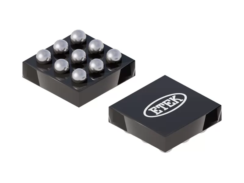
Designing a compact, high-efficiency buck boost converter circuit is essential whenever a regulated system rail—such as 3.3V or 3.5V—must operate continuously across an input voltage range that swings both above and below the target output voltage. A freshly charged single-cell lithium-ion (Li-ion) or lithium-polymer (LiPo) battery starts between 4.2V and 4.45V (VIN > VOUT), crosses directly through the 3.3V–3.5V regulation zone during mid-discharge (VIN ≈ VOUT), and continues delivering usable energy down to 2.7V or even 2.2V under pulsed loads (VIN < VOUT).
To unlock the full battery discharge curve in space-constrained hardware, ETEK Microelectronics engineered the ET80101, an ultra-low-quiescent-current (< 5 µA), 1A synchronous buck-boost DC-DC converter with a 1 MHz I²C interface in a 1.28 mm × 1.28 mm WLCSP9 package.
In this article you will learn:
- Why single-cell Li-ion systems need a non-inverting buck boost converter circuit
- Three classic design hurdles in single-inductor buck-boost topologies
- How the ET80101 achieves seamless 3-mode transitions, < 5 µA IQ, and 1 MHz I²C voltage scaling
- Practical layout and inductor selection rules for WLCSP9 designs
What Is a Buck Boost Converter Circuit?
A non-inverting synchronous buck boost converter circuit is a DC-DC switching regulator that uses four internal MOSFET switches arranged around a single power inductor to step input voltages down (Buck mode), up (Boost mode), or regulate smoothly when input and output voltages are nearly equal (Buck-Boost mode). This allows a fixed 3.3V or 3.5V load to run across the entire voltage range of a discharging battery.
Three Challenges in Single-Inductor Buck-Boost Designs
1. Mode-Transition Ripple When VIN ≈ VOUT
In poorly controlled buck-boost ICs, operating near the crossover point where input voltage equals output voltage causes the controller to hunt repeatedly between step-down and step-up modes. This mode toggling injects low-frequency ripple onto the output rail, disturbing sensitive ADCs, fingerprint sensors, and optical modules.
2. Light-Load Battery Drain
Portable and wearable electronics spend most of their lifecycle in idle or sleep states drawing microamperes. If the buck-boost controller consumes tens of microamperes of quiescent current (IQ), standby battery runtime drops sharply.
3. Output Leakage in Shutdown
Conventional boost stages contain an intrinsic conduction path from input to output through the high-side synchronous rectifier body diode. Without true load disconnect, disabling the regulator fails to isolate downstream loads from the battery.
How the ET80101 Optimizes the Buck Boost Converter Circuit
The ET80101 addresses each of these limitations through a high-frequency (> 1 MHz) synchronous architecture that integrates all power switches, loop compensation, soft-start, and digital control into a wafer-level chip-scale package.
Seamless 3-Mode Transitions (Buck, Buck-Boost, and Boost)
Across its 2.2V to 5.0V input voltage range, the ET80101 delivers up to 1A of continuous output current while automatically selecting among three operating regimes:
- Buck Mode (VIN > VOUT): Steps down high battery voltages with minimal switching losses.
- Novel Buck-Boost Mode (VIN ≈ VOUT): Bridges the crossover region smoothly when input voltage approaches output voltage.
- Boost Mode (VIN < VOUT): Steps up deeply discharged battery voltages down to 2.2V, preventing premature system resets during peak current bursts.
Mode transitions occur at strictly defined thresholds, eliminating unwanted mode toggling in the VIN ≈ VOUT crossover zone and keeping output voltage ripple low. The converter also supports forward and reverse current operation with dedicated forward and backward current limits.
< 5 µA Quiescent Current with Auto-PFM and Forced PWM Modes
To maximize battery runtime in wearable devices and smart locks, the ET80101 draws less than 5 µA of operating quiescent current and less than 1 µA in shutdown. Engineers can select between two switching modes via I²C:
- Automatic PFM (Pulse Frequency Modulation) Mode: Automatically enters pulse-skipping at light loads to maintain high efficiency across the entire load range.
- Forced PWM (FPWM) Mode: Maintains continuous fixed-frequency switching (> 1 MHz) across all load currents for deterministic spectral performance and minimal output ripple.
Hardware VSEL Defaults Plus 1 MHz I²C Dynamic Voltage Scaling
At power-up—before the host MCU initializes its I²C bus—the VSEL pin sets both the default hardware output voltage and the 7-bit I²C slave address, allowing two ET80101 regulators to share the same I²C bus without an external multiplexer:
| VSEL Pin State | Default Hardware Output Voltage (VOUT) | 7-Bit I²C Slave Address (Binary) | 7-Bit I²C Slave Address (Hex) |
|---|---|---|---|
| VSEL = High (H) | 3.5V | 1110101 | 0x75 |
| VSEL = Low (L) | 3.3V | 1110110 | 0x76 |
Once running, the host processor can communicate over the High-Speed Plus Mode I²C interface (up to 1 MHz) to:
- Program VOUT from 2.025V to 5.2V in fine 25 mV/step increments
- Control output voltage transition slew rate during dynamic voltage scaling (DVS)
- Select Auto-PFM or FPWM mode on the fly
- Manage software startup/shutdown, status flags, and Power Good (PG) signaling
True Load Disconnect, 500 µs Soft-Start, and Full Protection
Unlike standard boost converters, the ET80101 implements True Load Disconnect during shutdown, isolating the output rail from the input battery. When disabled, an integrated active discharge circuit bleeds the output capacitance to ground within 20 ms.
During turn-on, an internal fixed 500 µs soft-start limits battery inrush current. Fault protection includes cycle-by-cycle current limit, hiccup short-circuit protection, non-latching under-voltage protection (UVP), and thermal shutdown (TSD).
ET80101 Key Specifications
| Parameter | ET80101 Specification | System Design Benefit |
|---|---|---|
| Input Voltage Range (VIN) | 2.2V to 5.0V | Extracts full usable capacity from single-cell Li-ion/LiPo batteries |
| Programmable Output Voltage (VOUT) | 2.025V to 5.2V (25 mV/step via I²C) | Covers 2.5V, 3.0V, 3.3V, 3.5V, and 5.0V rails with one BOM item |
| Hardware Default VOUT | 3.5V (VSEL = H) / 3.3V (VSEL = L) | Autonomous boot before MCU I²C initialization |
| Continuous Output Current (IOUT) | Up to 1A | Drives high-current pulsed loads (optical modules, RF PA, sensors) |
| Switching Frequency (fSW) | > 1 MHz | Enables compact low-profile inductors and tiny MLCCs |
| Operating Quiescent Current (IQ) | < 5 µA | Extends standby battery life in wearables and IoT nodes |
| Shutdown Current | < 1 µA (with True Load Disconnect) | Isolates load completely when powered off |
| Soft-Start / Active Discharge | 500 µs soft-start / 20 ms discharge | Prevents startup brownouts and ensures clean rail reset |
| Digital Interface | 1 MHz I²C (0x75 / 0x76 via VSEL) | Dynamic voltage scaling, mode control, status flags, and PG output |
| Package | WLCSP9 (1.28 mm × 1.28 mm, 0.4 mm pitch) | Ultra-compact footprint for space-constrained PCB layouts |
Typical Applications
- Compact Wearable Devices: Smartwatches, fitness bands, AR/VR glasses, and medical patches where single-cell LiPo voltage drops below 3.3V during pulsed LED or wireless transmission loads.
- Voltage Stabilizers: Datacom equipment, optical transceiver modules, and thermoelectric cooling/heating (TEC) stages.
- System Pre-Regulators: Smartphones, tablets, POS terminals, and telematics units experiencing battery voltage sag during RF bursts.
- Point-of-Load (PoL) Regulation: Wired industrial sensors, port/cable adapters, and dongles compensating for cable IR drop.
- Fingerprint and Camera Sensors: Electronic smart door locks and IP network cameras requiring stable 3.3V or 3.5V sensor power across battery discharge states.
For higher-voltage step-down requirements, see our related article on the ETEK ET81313 17V 3A synchronous buck converter in SOT563.
PCB Layout Tips for WLCSP9 Buck-Boost Circuits
- Minimize Both Input and Output Switching Loops: Because a buck boost converter circuit switches discontinuous currents on the input side in Buck mode and on the output side in Boost mode, place low-ESR X5R/X7R ceramic decoupling capacitors immediately adjacent to the VIN, VOUT, and GND bumps of the WLCSP9 package.
- Keep Switching Nodes Compact: Place the power inductor as close as possible to the SW1 and SW2 pins using short, wide copper traces on the top layer.
- Isolate Digital Control Lines: Route the 1 MHz I²C lines (SDA, SCL) and VSEL away from the inductor switching nodes to prevent capacitive noise coupling.
- Size Inductor Saturation Current for Low-VIN Boost Operation: Ensure the inductor’s saturation current rating exceeds peak inductor current at minimum input voltage (2.2V) and full 1A output load.
Frequently Asked Questions
Why use a buck boost converter circuit instead of a standard buck converter for a single-cell Li-ion battery?
A single-cell Li-ion battery discharges from 4.2V–4.45V down to 2.7V–2.5V and may momentarily dip toward 2.2V under heavy current pulses or cold temperatures. A buck converter loses regulation as soon as VIN falls near 3.4V, leaving 20% to 35% of battery capacity unused. The ET80101 buck boost converter circuit regulates seamlessly down to 2.2V, extracting the full usable charge.
Can the ET80101 operate without I²C software programming?
Yes. While the 1 MHz I²C interface unlocks dynamic voltage scaling from 2.025V to 5.2V (in 25 mV steps) and mode selection, the ET80101 boots autonomously using its hardware VSEL pin: tying VSEL Low outputs 3.3V (0x76), and tying VSEL High outputs 3.5V (0x75).
Can two ET80101 buck-boost regulators share the same I²C bus?
Yes. Because the VSEL pin configures two distinct 7-bit I²C slave addresses—0x75 (1110101) when VSEL = High and 0x76 (1110110) when VSEL = Low—two ET80101 devices can connect directly to the same SDA/SCL bus and be programmed independently after startup.
What happens to the output rail when the ET80101 is shut down?
When disabled, the ET80101 activates True Load Disconnect to isolate the output from the input supply (< 1 µA shutdown current) and engages an internal active discharge switch that discharges the output rail to ground within 20 ms.
Conclusion: Full Battery Utilization in a 1.28 mm × 1.28 mm Footprint
For single-cell Li-ion wearables, smart locks, and optical modules, the ET80101 delivers a complete 1A synchronous buck boost converter circuit with seamless 3-mode transitions, < 5 µA quiescent current, and 1 MHz I²C programmability in an ultra-compact WLCSP9 package.
👉 Visit the ET80101 product page and explore ETEK’s DC-DC converter portfolio
✉️ Request Sample: https://www.etekmicro.com/sample


