
 EN


Logic Gate Circuit Design Guide: High-Drive 1.65V–5.5V OR Gate Implementation with the AEC-Q100 Qualified ETQ74LVC1G32
 2026/11/05
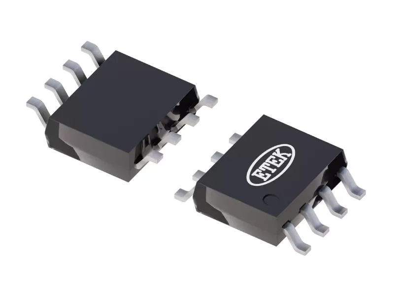
A logic gate circuit forms the foundational decision-making block of digital hardware, combining binary input signals to control power sequencing, interrupt aggregation, clock gating, and safety interlocks without burdening a host microcontroller or FPGA. While multi-gate quad IC packages once dominated board design, modern high-density automotive and industrial PCBs increasingly rely on single-gate (“1G”) CMOS logic placed directly at the point of signal routing to eliminate long trace stubs, reduce crosstalk, and bridge mismatched voltage domains.
To support rugged, space-constrained digital interfaces, ETEK Microelectronics engineered the ETQ74LVC1G32, an Automotive AEC-Q100 Grade 1 qualified single 2-input positive OR gate operating from 1.65V to 5.5V with 5.5V over-voltage tolerant inputs, ±32 mA balanced output drive, and ultra-compact SC70-5 and SOT23-5 packages.
In this article you will learn:
- How a 2-input OR logic gate circuit operates and its truth table behavior
- Four common hardware pitfalls in mixed-voltage and automotive logic designs
- How the ETQ74LVC1G32 delivers LCX-class speed and ±32 mA drive across -40°C to +125°C
- Four practical circuit topologies and PCB layout rules for high-speed CMOS logic
What Is an OR Logic Gate Circuit?
An OR logic gate circuit is a combinational digital switch that implements logical disjunction (Y = A + B). Its output (Y) switches to a logic HIGH state whenever at least one of its inputs (A or B) is asserted HIGH, and pulls LOW only when all inputs are LOW simultaneously. In hardware design, single 2-input OR gates are widely used to combine active-high wake-up events, merge fault flags, gate enable signals, and buffer weak digital outputs across 1.8V, 2.5V, 3.3V, and 5.0V power rails.
| Input A | Input B | Output Y (Y = A + B) | Functional State |
|---|---|---|---|
| L (Low) | L (Low) | L (Low) | Output driven LOW only when both inputs are LOW |
| L (Low) | H (High) | H (High) | Input B asserts output HIGH |
| H (High) | L (Low) | H (High) | Input A asserts output HIGH |
| H (High) | H (High) | H (High) | Both inputs active; output remains HIGH |
Four Hardware Challenges in Modern Logic Gate Circuits
1. Back-Powering During Partial Power-Down
Embedded systems frequently divide power rails into always-on standby domains and switched active domains. Standard CMOS logic inputs contain upper ESD clamping diodes tied to the VCC rail. If a 3.3V or 5.0V signal drives the input of a logic gate whose VCC supply is powered down (VCC = 0V), current flows through the upper clamp diode into the unpowered supply rail—wasting battery power and causing erratic latch-up or brownout resets.
2. Mixed-Voltage Interfacing Between 5V Sensors and Low-Voltage SoCs
Industrial and automotive boards routinely combine 5.0V CAN/LIN transceivers or legacy Hall sensors with 3.3V or 1.8V microcontrollers. A standard logic gate powered from 1.8V or 3.3V cannot accept a 5.0V input signal unless its input stage is specifically engineered without a positive rail clamp to VCC.
3. Insufficient GPIO Drive Strength for Capacitive Loads
Advanced process-node MCUs and SoCs often restrict GPIO source and sink currents to 2 mA–8 mA. Driving long board traces, optocouplers, indicator LEDs, or multiple fan-out loads directly from a weak MCU pin degrades rise and fall times (tr, tf) and increases propagation delay skew.
4. Thermal and ESD Stress in Automotive Environments
Body control modules, in-cabin infotainment units, and industrial controllers must operate reliably up to +125°C ambient temperature while surviving severe electrostatic discharge (ESD) and supply latch-up events. Commercial-grade logic gates rated only to +85°C lack the qualification margin required for automotive electronics.
How the ETQ74LVC1G32 Optimizes Logic Gate Circuit Design
The ETQ74LVC1G32 is fabricated in an advanced low-voltage CMOS (LVC) technology that matches the speed and output drive of multi-gate LCX families while occupying a fraction of the PCB area.
Wide 1.65V to 5.5V Supply with 5.5V Over-Voltage Tolerant Inputs
The ETQ74LVC1G32 operates across a continuous supply voltage range of 1.65V to 5.5V (with data retention down to 1.5V). Crucially, both inputs (A and B) are over-voltage tolerant up to 5.5V independent of the operating VCC level.
This allows a logic gate circuit powered from a 1.8V, 2.5V, or 3.3V rail to accept higher-voltage logic signals (up to 5.5V) directly on its inputs, functioning as a clean high-to-low voltage translator and logic combiner in a single device. Furthermore, during power-off conditions (VCC = 0V), the power-off leakage current (IOFF) with VI or VO = 5.5V is restricted to just 1.0 µA typical (10 µA maximum across -40°C to +125°C), preventing back-biasing in partial-power-down architectures.
±32 mA Balanced Output Sink and Source Capability
Unlike low-drive logic gates, the ETQ74LVC1G32 features a symmetrical push-pull output stage capable of sourcing and sinking up to ±32 mA at VCC = 4.5V and ±24 mA at VCC = 3.0V:
- VCC = 4.5V (IOH = -32 mA / IOL = 32 mA): VOH = 4.0V typical (3.8V min); VOL = 0.42V typical (0.55V max)
- VCC = 3.0V (IOH = -24 mA / IOL = 24 mA): VOH = 2.5V typical (2.3V min); VOL = 0.38V typical (0.55V max)
- VCC = 2.7V (IOH = -12 mA / IOL = 12 mA): VOH = 2.4V typical (2.2V min); VOL = 0.22V typical (0.40V max)
- VCC = 2.3V (IOH = -8 mA / IOL = 8 mA): VOH = 2.1V typical (1.9V min); VOL = 0.20V typical (0.30V max)
- VCC = 1.65V (IOH = -4 mA / IOL = 4 mA): VOH = 1.52V typical (1.29V min); VOL = 0.08V typical (0.24V max)
High-Speed Propagation Delay and Near-Zero Static Power
As specified in the ETQ74LVC1G32 Datasheet (Rev 1.7.c), propagation delay (tPD) from input A or B to output Y is just 4.9 ns typical at VCC = 4.5V–5.5V and 6.7 ns typical at VCC = 3.0V–3.6V driving a standard 50 pF / 500 Ω load.
When inputs are held static at VCC or GND, quiescent supply current (ICC) is only 1.0 µA typical at 25°C (10 µA maximum across -40°C to +125°C), and input capacitance (CIN) is just 2.5 pF typical, minimizing capacitive loading on upstream buses.
Automotive AEC-Q100 Grade 1 Qualification
The ETQ74LVC1G32 is fully qualified to Automotive AEC-Q100 Grade 1 standards for operation across -40°C to +125°C ambient temperature (TJ up to 150°C), backed by rigorous component-level stress testing:
- ESD Human Body Model (HBM): ±4000V Pass per AEC-Q100-002 (JEDEC JS-001)
- ESD Charged Device Model (CDM): ±1000V Pass per AEC-Q100-011 (JEDEC JS-002)
- Latch-Up Immunity (ILU): ±100 mA Pass at 125°C per AEC-Q100-004 (JEDEC JESD78F)
ETQ74LVC1G32 Key Specifications and Package Options
| Parameter | Test Conditions | ETQ74LVC1G32 Specification | Engineering Benefit |
|---|---|---|---|
| Logic Function | Single 2-Input Positive OR Gate | Y = A + B | Compact point-of-use signal combining |
| Operating Supply (VCC) | Continuous / Data Retention | 1.65V to 5.5V (1.5V retention) | Covers 1.8V, 2.5V, 3.3V, and 5.0V rails |
| Input Voltage Tolerance (VI) | Independent of VCC | 0V to 5.5V (-0.5V to 6.5V abs. max) | Direct high-to-low voltage level translation |
| Balanced Output Drive (IOH/IOL) | VCC = 4.5V / VCC = 3.0V | ±32 mA / ±24 mA | Drives long PCB traces, LEDs, and heavy loads |
| Quiescent Current (ICC) | VCC = 5.5V, VI = 5.5V or GND | 1.0 µA typ (25°C) / 10 µA max (125°C) | Near-zero standby battery drain |
| Power-Off Leakage (IOFF) | VCC = 0V, VI or VO = 5.5V | 1.0 µA typ (25°C) / 10 µA max (125°C) | Prevents back-powering in sleep domains |
| Propagation Delay (tPD) | CL = 50 pF, RL = 500 Ω | 4.9 ns typ (5V) / 6.7 ns typ (3.3V) | Fast response for timing-critical gating |
| Input / Power Dissipation Cap. | CIN / CPD (f = 10 MHz) | 2.5 pF typ / 21 pF typ | Low dynamic switching power dissipation |
| Automotive Qualification | AEC-Q100 Grade 1 | -40°C to +125°C; HBM ±4 kV, CDM ±1 kV | Validated for automotive body & cabin systems |
To fit both ultra-dense modules and automated optical inspection (AOI) assembly lines, ETEK offers two Moisture Sensitivity Level 1 (MSL 1), Pb-free, RoHS-compliant 5-pin packages sharing the same industry-standard pinout (Pin 1: A, Pin 2: B, Pin 3: GND, Pin 4: Y, Pin 5: VCC):
| Part Number | Package Type | Body Dimensions | Lead Pitch | Packing Option | MSL Rating |
|---|---|---|---|---|---|
| ETQ74LVC1G32 | SC70-5 | 1.3 mm × 2.1 mm (Max height 1.10 mm) | 0.65 mm BSC | Tape & Reel, 3,000 pcs/reel | MSL 1 |
| ETQ74LVC1G32T | SOT23-5 | 1.6 mm × 2.9 mm (RθJA = 250°C/W) | 0.95 mm NOM | Tape & Reel, 3,000 pcs/reel | MSL 1 |
Four Practical Logic Gate Circuit Applications
1. Multi-Source Wake-Up and Interrupt Aggregation
In automotive body electronics and battery-powered IoT nodes, an MCU often sleeps until woken by either a CAN/LIN transceiver wake signal (WAKE_A) or a local user button / Hall switch event (WAKE_B). Combining both active-high signals through an ETQ74LVC1G32 OR gate lets either event assert a single MCU wake-up pin while isolating the two sources from one another.
2. Hardware Safety Interlock and Enable Gating
Power regulators, motor drivers, and laser drivers frequently require an active-high enable (EN) that stays asserted if either the primary host MCU requests operation (MCU_EN) or a hardware keep-alive timer (HOLD_EN) is active during firmware reboot. Placing an ETQ74LVC1G32 directly at the regulator’s EN pin ensures glitch-free power-rail holdover without external diode OR-ing voltage drops.
3. Down-Translation from 5V Logic to 3.3V or 1.8V Inputs
Because the inputs of the ETQ74LVC1G32 tolerate up to 5.5V regardless of supply voltage, powering the gate’s VCC pin from the target 3.3V or 1.8V MCU rail allows 5.0V digital sensor outputs to be combined and shifted down to 3.3V or 1.8V CMOS levels in one step.
4. High-Current Line Buffering
By tying inputs A and B together (or tying one input to GND), the ETQ74LVC1G32 acts as a non-inverting ±32 mA buffer that restores crisp signal edges and drives high-capacitance backplane traces or status LEDs. For multi-channel bus buffering or inverting logic, explore our articles on ET74LV541V octal buffers and line drivers and ET74LVC04A logic inverter circuits.
PCB Layout and Design Guidelines for LVC Logic Gates
- Tie All Unused Inputs to a Valid Logic Level: Never leave CMOS inputs floating. If only one input of the OR gate is used as a non-inverting buffer, tie the second input directly to GND (or tie A and B together) so the input stage cannot oscillate near the switching threshold and draw excess shoot-through current.
- Observe Input Transition Slew-Rate Limits (tr, tf): To prevent output oscillation on slow RC-filtered signals, keep input rise and fall times within the datasheet’s recommended limits: ≤ 20 ns/V at VCC = 2.5V, ≤ 10 ns/V at VCC = 3.0V, and ≤ 5 ns/V at VCC = 5.0V.
- Place Local Supply Decoupling Close to Pin 5 (VCC): Because the ±32 mA output stage switches in a few nanoseconds, place a 0.1 µF low-ESR X7R ceramic bypass capacitor within 2 mm of Pin 5 (VCC) and Pin 3 (GND) to suppress supply bounce.
- Budget Dynamic Power at High Switching Frequencies: Use the datasheet’s power dissipation capacitance (CPD = 21 pF) to calculate dynamic power when toggling at megahertz rates: PD = CPD × VCC² × fi × N + Σ(CL × VCC² × fo).
Frequently Asked Questions
Can the ETQ74LVC1G32 accept 5V input signals when powered from a 3.3V or 1.8V supply?
Yes. The ETQ74LVC1G32 features over-voltage tolerant inputs rated up to 5.5V independent of its operating supply voltage (VCC = 1.65V to 5.5V). You can drive inputs A and B with 5.0V logic signals while powering VCC at 3.3V or 1.8V to translate the output Y down to the lower rail.
What happens to the ETQ74LVC1G32 inputs and output when VCC is 0V?
When VCC = 0V, the ETQ74LVC1G32 enters a high-impedance power-off state. With up to 5.5V applied to the inputs or output, power-off leakage current (IOFF) is limited to 1.0 µA typical at 25°C (10 µA maximum across -40°C to +125°C), preventing active signals from back-powering a powered-down subsystem.
Is the ETQ74LVC1G32 qualified for automotive electronics?
Yes. Both the SC70-5 (ETQ74LVC1G32) and SOT23-5 (ETQ74LVC1G32T) packages are Automotive AEC-Q100 Grade 1 qualified for ambient temperatures from -40°C to +125°C, passing ±4000V HBM ESD (AEC-Q100-002), ±1000V CDM ESD (AEC-Q100-011), and ±100 mA latch-up testing at 125°C (AEC-Q100-004).
How should I choose between the SC70-5 and SOT23-5 packages?
Both packages share the exact same 5-pin configuration and electrical performance. Choose the SC70-5 (ETQ74LVC1G32, 1.3 mm × 2.1 mm) when minimizing PCB footprint in compact modules or wearables is the priority. Choose the SOT23-5 (ETQ74LVC1G32T, 1.6 mm × 2.9 mm) when wider 0.95 mm lead pitch simplifies routing and solder-joint inspection.
Conclusion: Compact, Automotive-Grade Logic Where You Need It
For engineers designing mixed-voltage interfaces, wake-up combiners, and safety gating in automotive and industrial hardware, the ETQ74LVC1G32 delivers a fast, high-drive logic gate circuit with 1.65V–5.5V operation, 5.5V-tolerant inputs, and AEC-Q100 Grade 1 reliability.
👉 Visit the ETQ74LVC1G32 product page, download the ETQ74LVC1G32 datasheet, or browse ETEK’s Digital Logic Gate IC portfolio
✉️ Request Sample: https://www.etekmicro.com/sample


