
 EN


4-Bit Level Shifter for I2C, I3C, and SPI: Auto-Bidirectional 0.95V–5.0V Voltage Translation with the ETEK ETF0104
 2026/11/06
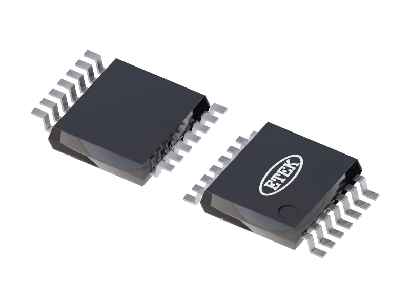
A 4-bit level shifter for I2C and multi-signal peripheral buses is essential whenever a low-voltage host processor—operating at 0.95V, 1.2V, or 1.8V core I/O—must communicate reliably with legacy 3.3V or 5.0V sensors, EEPROMs, power management ICs, and communication transceivers. As modern SoCs and FPGAs shrink transistor geometries to reduce power consumption, their I/O banks can no longer tolerate 3.3V or 5.0V pull-up voltages directly, while peripheral devices still require higher logic thresholds for noise immunity.
To bridge these voltage domains without software direction control or bulky discrete MOSFET arrays, ETEK Microelectronics developed the ETF0104, a 4-channel auto-bidirectional multi-voltage level translator that supports both open-drain (I²C, I3C, MDIO, SMBus) and push-pull (SPI, UART, I2S, SDIO, DMIC, GPIO) interfaces across 0.95V–3.3V to 1.62V–5.0V at data rates up to 40 MHz.
In this article you will learn:
- Why mixed-voltage I²C, I3C, and SPI buses need an auto-bidirectional 4-bit level shifter
- How the ETF0104’s low-RON pass-switch architecture translates signals up and down without a DIR pin
- How to calculate pull-up resistor values for maximum data rate and safe sink current
- Package options (TSSOP14, 2.0 mm × 1.7 mm QFN12, 1.6 mm × 1.6 mm QFN12) and PCB layout guidelines
What Is a 4-Bit Level Shifter for I2C and Multi-Signal Interfaces?
A 4-bit level shifter for I2C is a four-channel bidirectional voltage translator IC that converts digital logic levels between a low-voltage port (A1–A4, referenced to REF_A) and a higher-voltage port (B1–B4, referenced to REF_B). Because it integrates four independent auto-direction channels in a single package, one IC can translate two separate I²C buses (SDA1/SCL1 and SDA2/SCL2), an I²C bus plus two interrupt/reset GPIOs, or a complete 4-wire SPI / UART / I2S interface without requiring a direction-control pin from the host MCU.
Three Engineering Challenges in Mixed-Voltage Bus Translation
1. Direction Reversal Without a Hardware DIR Pin
Protocols such as I²C, I3C, MDIO, and SDIO transfer data bidirectionally on the same wire—for example, when a peripheral pulls SDA LOW to send an ACK bit immediately after the controller transmits an address byte. Direction-controlled level shifters cannot switch fast enough without dedicated direction signaling, while buffered one-shot translators often struggle when driving both open-drain and push-pull loads on the same IC.
2. Signal Integrity Loss from High RON and Channel Skew
Discrete MOSFET level shifters and high-impedance translators introduce tens of ohms of series resistance and mismatched channel delays. In high-speed interfaces such as 40 MHz SPI, I3C, or I2S audio clocks, excessive on-resistance (RON) increases the low-level output voltage (VOL) and degrades noise margin, while channel-to-channel skew (tsk) corrupts setup and hold timing between clock and data lines.
3. Board Space and Routing Congestion in Compact Hardware
Implementing four bidirectional level-shifting channels with discrete SOT-23 MOSFETs and eight pull-up resistors consumes significant PCB area and forces crisscrossing trace stubs. Compact servers, personal computers, industrial controllers, and wearable hubs require a flow-through pinout in millimeter-scale packages.
How the ETF0104 4-Bit Level Shifter Works
The ETF0104 uses a voltage-clamped pass-transistor switch architecture controlled by two reference supply pins—REF_A (VCCA, the low-voltage side from 0.95V to 3.3V) and REF_B (VCCB, the high-voltage side from 1.62V to 5.0V)—plus an active-high enable input (EN).
Seamless Up-Translation and Down-Translation Logic
As detailed in the ETF0104 Datasheet (Rev 1.3), each channel (An ↔ Bn) automatically adjusts its switch state based on the instant voltage on the ports:
| Signal Direction | Input State | Pass Switch State | Electrical Functionality |
|---|---|---|---|
| B to A (Down-Translation) | Bn = LOW | ON (Low Impedance) | An port is pulled LOW through the low-RON switch to match the Bn port voltage |
| B to A (Down-Translation) | Bn = HIGH | OFF (High Impedance) | Switch turns OFF; An port voltage is safely clamped at VREF_A |
| A to B (Up-Translation) | An = LOW | ON (Low Impedance) | Bn port is pulled LOW through the low-RON switch to match the An port voltage |
| A to B (Up-Translation) | An = HIGH | OFF (High Impedance) | Switch turns OFF; Bn port is pulled up to the high-side pull-up supply (VPU) |
When EN = LOW, all four data channels enter a high-impedance (Hi-Z) state, isolating the A-side and B-side buses during power sequencing or standby while drawing just 0.01 µA typical (2 µA maximum) shutdown current. For always-enabled operation, EN can be tied directly to REF_A.
Ultra-Low 3.0 Ω On-State Resistance (RON) for Minimal Distortion
When either side pulls a line LOW, the ETF0104 provides an exceptionally low-resistance conduction path capable of passing up to 64 mA continuous pass-transistor current (IPASS, with 100 mA absolute maximum rating):
- VCCA = 3.3V, VCCB = 5.0V (VI = 0V, IO = 64 mA): RON = 3.0 Ω typical (7.0 Ω maximum)
- VCCA = 2.5V, VCCB = 5.0V (VI = 0V, IO = 32 mA): RON = 3.0 Ω typical (8.0 Ω maximum)
- VCCA = 1.8V, VCCB = 3.3V (VI = 0V, IO = 3 mA): RON = 3.71 Ω typical (10 Ω maximum)
- VCCA = 1.2V, VCCB = 3.3V (VI = 0V, IO = 3 mA): RON = 4.52 Ω typical (10 Ω maximum)
- VCCA = 1.0V, VCCB = 5.0V (VI = 0V, IO = 64 mA): RON = 5.0 Ω typical (10 Ω maximum)
This low RON keeps the voltage drop across the translator negligible during I²C ACK pulses and high-speed push-pull transitions, preserving full VIL noise margin across both sides of the bus.
Up to 40 MHz Data Rate and Sub-Nanosecond Propagation Delay
Because the ETF0104 is a passive-switch translator without internal latching buffers, propagation delay through the switch is extremely short, and channel-to-channel skew (tsk) is just 0.2 ns typical (0.5 ns maximum):
- Down-Translation (3.3V → 1.8V, CL = 20 pF): tPLH = 0.3 ns typical (1.2 ns max); tPHL = 0.4 ns typical (2.0 ns max)
- Down-Translation (5.0V → 3.3V, CL = 20 pF): tPLH = 0.8 ns typical (1.2 ns max); tPHL = 0.4 ns typical (1.5 ns max)
- Up-Translation (1.8V → 3.3V, CL = 20 pF): tPLH = 0.6 ns typical (1.0 ns max); tPHL = 1.2 ns typical (3.0 ns max)
- Up-Translation (1.2V → 1.8V, CL = 20 pF): tPLH = 1.1 ns typical (1.5 ns max); tPHL = 1.7 ns typical (3.0 ns max)
- Maximum Transmission Frequency (fMAX):40 MHz minimum (RUP = 100 Ω, CL = 30 pF), easily covering Standard/Fast/Fast-Mode Plus I²C, I3C, MDIO, UART, I2S, and SPI interfaces.
ETF0104 Key Specifications and Package Comparison
| Parameter | Test Conditions | ETF0104 Specification (Typ / Max) | System Design Benefit |
|---|---|---|---|
| Channels | Auto-bidirectional (A1–A4 ↔ B1–B4) | 4 Channels (No DIR pin required) | Translates 2× I²C buses or 1× 4-wire SPI/UART bus |
| Low-Side Supply (REF_A) | VCCA (Lowest voltage in system) | 0.95V to 3.3V (0.9V–5.5V operating) | Interfaces directly with sub-1V and 1.2V/1.8V SoCs |
| High-Side Supply (REF_B) | VCCB (VCCB ≥ VCCA + 0.8V) | 1.62V to 5.0V (up to 5.5V operating) | Supports 1.8V, 2.5V, 3.3V, and 5V TTL/CMOS buses |
| On-State Resistance (RON) | VCCA = 3.3V, VCCB = 5V, IO = 64 mA | 3.0 Ω typ / 7.0 Ω max | Minimal VOL offset and signal distortion |
| Max Transmission Rate (fMAX) | RUP = 100 Ω, CL = 30 pF | 40 MHz | Supports I²C, I3C, SPI, MDIO, UART, I2S, SDIO |
| Channel-to-Channel Skew (tsk) | CL = 20 pF / 50 pF | 0.2 ns typ / 0.5 ns max | Preserves clock-to-data timing in synchronous buses |
| Standby / Shutdown Current | ICC (EN = H) / Ioff (EN = L) | 0.01 µA typ (5 µA / 2 µA max) | Near-zero static power consumption |
| I/O Capacitance | CIO(off) (EN = 0V) / CIO(on) (EN = 3V) | 4.0 pF typ / 12 pF typ | Low capacitive loading on I²C/I3C buses |
| ESD & Latch-Up Ratings | JEDEC JS-001 / JS-002 / JESD78F | ±2000V HBM, ±1000V CDM, >±100 mA LU | Industrial-grade robustness (-40°C to +85°C) |
All three ETF0104 package variants feature a flow-through pinout (A1–A4 on one side and B1–B4 on the opposite side) to simplify straight-line PCB trace routing:
| Part Number | Package Type | Body Dimensions | Pin Pitch | GND / REF_A / REF_B / EN Pins | A1–A4 / B1–B4 Pins | Packing & MSL |
|---|---|---|---|---|---|---|
| ETF0104V | TSSOP14 | 5.0 mm × 4.4 mm | 0.65 mm BSC | Pin 7 (GND), Pin 2 (REF_A), Pin 14 (REF_B), Pin 8 (EN) | Pins 3–6 (A1–A4) / Pins 10–13 (B1–B4) | 4K/Reel, MSL 3 |
| ETF0104Y1 | QFN12 | 2.0 mm × 1.7 mm | 0.40 mm TYP | Pin 6 (GND), Pin 1 (REF_A), Pin 11 (REF_B), Pin 12 (EN) | Pins 2–5 (A1–A4) / Pins 7–10 (B1–B4) | 3K/Reel, MSL 1 |
| ETF0104Y4 | QFN12 | 1.6 mm × 1.6 mm | 0.40 mm NOM | Pin 5 (GND), Pin 12 (REF_A), Pin 10 (REF_B), Pin 11 (EN) | Pins 1–4 (A1–A4) / Pins 6–9 (B1–B4) | 3K/Reel, MSL 1 |
(Note: On the TSSOP14 ETF0104V, Pins 1 and 9 are NC [Not Connected]. Refer to Figure 1 and the Pin Function table in the ETF0104 Datasheet when creating PCB footprints.)
Pull-Up Resistor Selection and PCB Design Guidelines
- Keep VCCA (REF_A) as the Lowest Supply Voltage:REF_A sets the internal switch clamping threshold and must always be connected to the lowest interface voltage (0.9V ≤ VCCA ≤ 5.5V), while REF_B connects to the higher supply (VCCB ≥ VCCA + 0.8V in standard bias configurations).
- Configure Pull-Up Resistors for Up- vs. Down-Translation:
- Up-Translation (A to B): Pull-up resistors (RB) to the high-side pull-up supply (VPU ≤ VCCB) are always required on the B-side because the pass switch turns OFF when An goes HIGH. Pull-up resistors on the A-side (RA) are only needed if the A-side driver is open-drain (such as I²C) or has input leakage exceeding 1 µA.
- Down-Translation Only (B to A with Push-Pull Driver): If a channel only translates downward from a push-pull B-side transmitter to a low-leakage (< 1 µA) CMOS A-side receiver, external pull-up resistors can be omitted on that channel.
- Balance Data Rate Against Driver Sink Current (IOL):
- Maximum data rate is governed by the B-side RC time constant during rising edges: fMAX ≈ 1 / (6 × RB1 × CB1)
- When pulling a line LOW, the active driver must sink the combined current from both pull-up resistors: IOL ≈ (VCCA / RA1) + (VCCB / RB1)
- For standard 400 kHz–1 MHz I²C buses, pull-up values between 1 kΩ and 4.7 kΩ provide clean rising edges while keeping sink current well within I²C driver limits; for high-speed multi-megahertz links, lower resistance values (down to 100 Ω–220 Ω) reduce rise time (tR ≈ 10 ns at RUP = 220 Ω, CL = 50 pF).
- Decouple REF_B and REF_A Locally: Place a 0.1 µF ceramic filter capacitor close to the REF_B and REF_A pins to stabilize the bias reference during fast multi-channel switching.
Need a 2-channel or 8-channel translator, or a dedicated SIM card interface? Explore the ETF0102 2-bit bidirectional level shifter, read our articles on the ETS0108 8-channel bidirectional level shifter and ET4559 SIM card level translator, or browse ETEK’s full Level Shifter IC product line.
Frequently Asked Questions
Why is the ETF0104 suitable as a 4-bit level shifter for I2C and I3C buses?
The ETF0104 uses a passive low-RON (3.0 Ω typical) switch architecture that supports both open-drain and push-pull signaling without a direction-control pin. Because it has no internal one-shot output driver that could cause bus contention during I²C ACK handshakes or I3C dynamic switching, signals flow bidirectionally with sub-nanosecond delay.
Can one ETF0104 translate both open-drain I2C lines and push-pull GPIO or SPI signals at the same time?
Yes. All four channels (A1–A4 ↔ B1–B4) operate independently between the shared REF_A and REF_B voltage domains. For example, two channels can translate an open-drain I²C bus (SDA, SCL) with pull-up resistors on both sides, while the remaining two channels translate push-pull interrupt, chip-select, or UART signals.
What is the minimum voltage supported by the ETF0104?
The low-voltage reference supply REF_A (VCCA) supports bidirectional translation down to 0.95V (with application operating conditions specified from 0.9V to 5.5V), while REF_B (VCCB) supports 1.62V to 5.0V (up to 5.5V). This allows direct translation between 1.0V/1.2V/1.8V core logic and 1.8V/2.5V/3.3V/5.0V peripherals.
How does the EN pin behave during power-up and power-down?
When the EN pin is pulled LOW (VIL(EN) ≤ 0.3 × VCCA), all four A-side and B-side I/O ports are placed into a high-impedance (Hi-Z) state and shutdown current drops to 0.01 µA typical. Pulling EN HIGH (VIH(EN) ≥ 0.7 × VCCA) or tying EN directly to REF_A enables bidirectional translation across all channels.
Conclusion: Flexible 4-Channel Voltage Translation in a Tiny Footprint
Whether you are bridging two I²C buses, an I3C sensor interface, or a 4-wire SPI link across 0.95V to 5.0V domains, the ETF0104 provides a low-distortion, directionless 4-bit level shifter for I2C and push-pull interfaces in TSSOP14 and ultra-compact QFN12 packages.
👉 Visit the ETF0104 product page, download the ETF0104 datasheet, or explore ETEK’s Level Shifter IC portfolio
✉️ Request Sample: https://www.etekmicro.com/sample


