
 EN


Current Limit Switch Design Guide: 80mΩ, 1.5A High-Side USB Power Protection with the ETEK ET20163
 2026/11/17
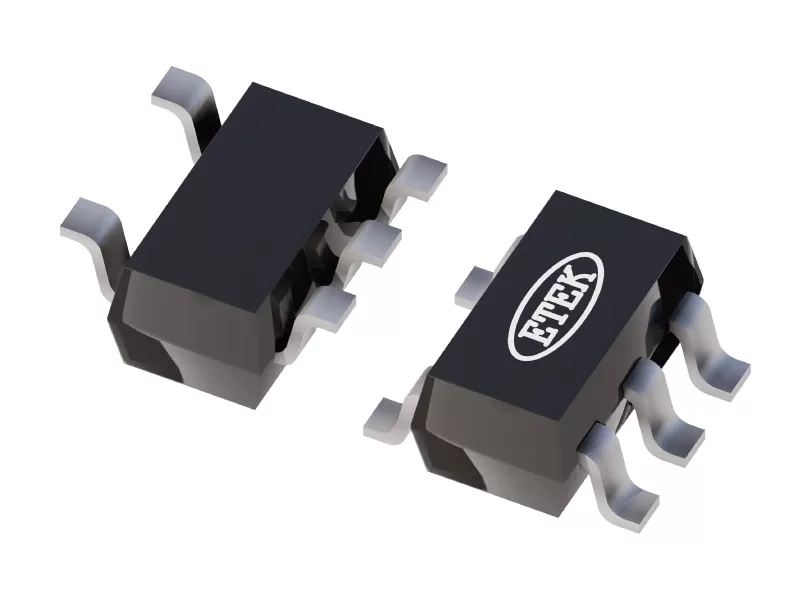
A current limit switch is an integrated high-side power distribution IC that combines a low on-resistance pass MOSFET with active current sensing, short-circuit clamping, thermal shutdown, and fault telemetry. Unlike a passive polyfuse (PPTC) or a basic discrete MOSFET switch, a current limit switch reacts within microseconds to clamp overload currents before a hot-plugged peripheral or shorted cable can pull down the upstream 3.3V or 5.0V system power rail.
To protect USB ports, notebook peripheral rails, smart TVs, and industrial embedded hosts without sacrificing voltage headroom or standby battery life, ETEK Microelectronics engineered the ET20163, a UL-listed (File No. E479717) P-channel MOSFET current limit switch operating from 2.5V to 5.5V with an 80 mΩ typical on-resistance (RDS(ON)), a 1.5A minimum fixed current limit, a 2 µs short-circuit response, true reverse current blocking, and a 25 µA typical quiescent current in a compact SOT23-5 package.
In this engineering guide, you will learn:
- Why hot-pluggable 3.3V and 5.0V power ports require an active current limit switch instead of a polyfuse
- How the ET20163 handles three distinct overload and short-circuit scenarios with a 2 µs response
- How the 6 ms deglitched FLT flag prevents false system resets during capacitive inrush events
- Step-by-step thermal dissipation calculations and PCB layout rules for reliable 1.5A power distribution
What Is a Current Limit Switch and Why Replace Discrete Polyfuses?
A current limit switch is a monolithic protection IC placed in series between a regulated power supply (IN) and an external load or connector (OUT). It continuously monitors load current through an internal sense FET and transitions smoothly from a low-impedance switch (80 mΩ) into a constant-current regulator whenever load demand exceeds the safe threshold.
In legacy board designs, engineers often paired a discrete P-channel MOSFET with a resettable polymeric positive temperature coefficient (PPTC) thermistor. However, PPTC polyfuses rely on joule heating (I²R) to trip, meaning:
- Slow Trip Time (Milliseconds to Seconds): During a dead short on a USB cable, a polyfuse allows tens of amperes to surge from the main 5V DC-DC converter before heating up, causing brownout resets across the host processor and memory subsystem.
- High Series Resistance and Voltage Drop: Even at normal operating current, polyfuses exhibit significant resistance that increases after every trip cycle, eating into the tight ±5% voltage tolerance of 5.0V USB VBUS rails.
- No Fault Telemetry or Reverse Blocking: A passive fuse cannot notify the host MCU when a port is overloaded, nor can it block reverse current when a self-powered peripheral remains energized while the host is powered down.
By integrating a precision sense FET, controlled soft-start gate drive, thermal cycling, reverse current blocking, and an open-drain fault flag (FLT) into a single SOT23-5 footprint, the ET20163 eliminates all three limitations.
Three Critical Power Distribution Challenges Solved by the ET20163
1. Hot-Plug Capacitive Inrush and Hard Short-Circuit Events
When a user plugs a USB hard drive, hub, or wireless dongle into an active port, the discharged bulk capacitance on the peripheral side appears momentarily as a near-zero-ohm load. Conversely, damaged connector pins can create a permanent dead short to ground. The ET20163 distinguishes between harmless startup charging and destructive faults by combining a controlled turn-on rise time (tR = 0.4 ms typical) with a 2 µs short-circuit response and a deglitched fault output.
2. Reverse Current Back-Drive into Unpowered Host Rails
In multi-supply systems, docking stations, and powered USB hubs, the output voltage (VOUT) can exceed the input voltage (VIN) when the host system enters sleep mode or shuts down while an external device remains powered. The ET20163 incorporates true reverse current blocking, limiting reverse leakage current (IREV) to just 0.2 µA typical (2 µA maximum when VOUT = 5V and VIN = 0V) to prevent back-feeding the upstream regulator.
3. Standby Power Budget in Battery-Powered Devices
Laptops, netbooks, smartphones, and portable instruments keep peripheral power switches enabled during idle states so connected keyboards, mice, or flash drives remain ready. The ET20163 draws only 25 µA typical quiescent current (IQ) when enabled at no load, and drops to 0.1 µA typical (1 µA maximum) in shutdown mode (VEN = 0V).
Inside the ET20163 Architecture and Overload Protection Mechanics
As documented in the ET20163 Datasheet (Rev 1.3), the IC integrates an 80 mΩ P-channel power MOSFET, an internal charge-pump/gate driver, an under-voltage lockout (UVLO) comparator, a current-sense FET (CS), a thermal sensor, a reverse-blocking block, and a 400 Ω typical output load discharge path.
SOT23-5 Pin Configuration and Functions
| Pin No. | Pin Name | I/O Type | Functional Description and Design Notes |
|---|---|---|---|
| 1 | OUT | Output | High-side protected power output; bypass close to pin (< 3 mm) with ceramic and bulk capacitance |
| 2 | GND | Ground | System ground reference; connect to a wide PCB copper plane for optimal heat dissipation |
| 3 | FLT | Output (Open-Drain) | Active-low over-current and over-temperature fault flag; pull up to ≤ 5.5V via a 1 kΩ to 100 kΩ resistor (10 kΩ typical) |
| 4 | EN | Input | Active-high enable control input (VIH ≥ 2.0V, VIL ≤ 0.8V); driving LOW disables switch and activates 400 Ω output discharge |
| 5 | IN | Power Input | Power supply input (2.5V to 5.5V operating range); decouple locally to GND with a 0.1 µF–1 µF ceramic capacitor |
How the ET20163 Responds to Three Overload Conditions
The ET20163 uses an internal sense FET to monitor load current continuously without requiring an external current-sense resistor. When an overload is detected, the control loop transitions the P-channel MOSFET into constant-current mode, holding output current at ILMT (1.5A min / 2.1A typ / 2.7A max) and reducing VOUT proportionally until the fault is cleared or thermal protection engages:
- Condition 1 — Output Shorted Before Enable or Power-Up: If OUT is already shorted to GND before EN is pulled HIGH or before VIN crosses the 1.8V typical UVLO threshold, the ET20163 senses the zero-impedance load during turn-on and immediately limits output current to the constant-current threshold without any current spike.
- Condition 2 — Sudden Short or Hot-Plug Overload While Enabled: If a dead short occurs while the switch is already fully ON, current briefly rises before the fast 2 µs short-circuit protection loop reacts and clamps the switch into constant-current mode, preventing upstream rail collapse.
- Condition 3 — Gradual Load Increase Beyond Rating: If downstream load current ramps up slowly past the recommended continuous operating current, the ET20163 allows current to rise until it reaches ILMT (or the thermal shutdown threshold), then smoothly regulates in constant-current mode without damaging the pass element.
Intelligent Fault Reporting (FLT) with Deglitch Blanking
To prevent nuisance microcontroller interrupts when charging downstream filter capacitors (CL), the open-drain FLT pin incorporates an internal 6 ms to 9 ms typical blanking timer (tFLT_BLANK = 2 ms min / 9 ms typ / 16 ms max) for over-current events:
- Transient Inrush (< Blanking Time): When a capacitive peripheral is plugged in, the switch briefly enters current limit to charge the capacitor. Because voltage recovers within a few milliseconds, FLT remains HIGH and no false fault is reported.
- Sustained Over-Current (> Blanking Time): If the current-limiting circuit remains active longer than the blanking period, an internal ~100 Ω pull-down FET asserts FLT LOW (VFLT_Lo ≤ 0.2V @ 1 mA sink) to alert the host controller.
- Over-Temperature Fault (Zero Delay): If die junction temperature reaches 150°C typical (130°C–165°C), FLT is pulled LOW immediately without deglitch delay while the switch turns OFF. Once the die cools by approximately 15°C to 25°C (thermal hysteresis), the switch automatically re-enables and cycles until the fault is removed.
Because FLT is an open-drain output rated up to 5.5V, it can be pulled up to an independent MCU I/O rail (such as 1.8V or 3.3V) even when the ET20163 is switching a 5.0V VBUS rail.
ET20163 Complete Electrical Specifications (VIN = 5.0V, TA = -40°C to +85°C)
All values below are taken directly from the official ET20163 Datasheet (Rev 1.3):
| Parameter | Symbol | Test Conditions | Min | Typ | Max | Unit |
|---|---|---|---|---|---|---|
| Input Voltage Range | VIN | Continuous operation | 2.5 | — | 5.5 | V |
| Input UVLO Threshold | VUVLO | Rising supply voltage | 1.4 | 1.8 | 2.3 | V |
| Active Quiescent Current | IQ | Enabled (VEN = VIN), IOUT = 0 mA | — | 25 | 60 | µA |
| Shutdown Supply Current | ISHDN | Disabled (VEN = 0V), OUT floating or shorted | — | 0.1 | 1.0 | µA |
| Switch On-Resistance | RDS(ON) | VIN = 5V, IOUT = 0.6A | — | 80 | 120 | mΩ |
| Fixed Current Limit | ILMT | VIN = 5V, VOUT = 4.5V | 1.5 | 2.1 | 2.7 | A |
| Short-Circuit Response Time | tIOS | Output shorted to GND | — | 2 | — | µs |
| Reverse Leakage Current | IREV | VOUT = 5V, VIN = 0V (measure IVOUT) | — | 0.2 | 2.0 | µA |
| Output Discharge Resistance | RDIS | VIN = 5V, VEN = 0V, VOUT = 5V | 200 | 400 | 800 | Ω |
| Turn-On Delay / Rise Time | tON / tR | VIN = 5V, CL = 1 µF, RL = 100 Ω | 0.2 / 0.1 | 0.5 / 0.4 | 1.0 / 0.7 | ms |
| Turn-Off Delay / Fall Time | tOFF / tF | VIN = 5V, CL = 1 µF, RL = 100 Ω | 0.1 / 0.05 | 0.5 / 0.23 | 0.9 / 0.40 | ms |
| FAULT Blanking Time | tFLT_BLANK | Over-current duration before FLT asserts LOW | 2 | 9 | 16 | ms |
| Thermal Shutdown / Hysteresis | TSHDN / THYS | VIN = 5V | 130 | 150 / 25 | 165 | °C |
| ESD & Safety Certification | — | HBM ESD / UL Recognition | — | 4 kV / UL E479717 | — | — |
Thermal Design Calculations and PCB Layout Guidelines
Checking Power Dissipation and Junction Temperature (TJ)
Because the ET20163 packs a high-current switch into a miniature SOT23-5 package (2.92 mm × 1.60 mm × 1.10 mm, thermal resistance RθJA = 250 °C/W on standard board copper), verifying normal-mode conduction loss is essential:
- Switch Conduction Power Dissipation (PD):PD = IOUT² × RDS(ON)
- Operating Junction Temperature (TJ):TJ = TA + (PD × RθJA)
For example, in a standard 5.0V USB port delivering 1.0A continuous current at an ambient temperature TA = 60°C using the typical RDS(ON) = 80 mΩ (0.08 Ω):
- PD = (1.0 A)² × 0.08 Ω = 0.08 W (80 mW, well below the 500 mW rating at 25°C)
- TJ = 60°C + (0.08 W × 250 °C/W) = 60°C + 20°C = 80°C (leaving a comfortable 70°C margin below the 150°C maximum junction temperature rating)
At 1.5A continuous load (PD = 1.5² × 0.08 Ω = 180 mW), the temperature rise is 45°C, keeping TJ = 105°C at TA = 60°C.
Four PCB Layout Best Practices for USB and 5V Rail Switching
To maximize transient immunity and thermal conductivity, follow the four EVB layout rules from the ET20163 Datasheet:
- Minimize High-Current Loop Area: Keep the high-current trace path from IN (Pin 5) to OUT (Pin 1) short and wide, and minimize the loop area formed by the input and output bypass capacitors.
- Place Output Capacitors Within 3 mm on the Same Layer: Mount the output ceramic bypass capacitor (0.01 µF to 1 µF) and bulk tantalum/electrolytic capacitor on the same PCB side as the ET20163, keeping the distance between the OUT pin and the output capacitor less than 3 mm to suppress inductive voltage ringing during short-circuit interruption.
- Decouple the IN Pin Locally: Place a 0.1 µF to 1 µF low-ESR ceramic capacitor directly adjacent to IN (Pin 5) and GND (Pin 2) to prevent input rail droop during load steps.
- Pour Generous Copper Areas on GND, IN, and OUT: Connect IN, OUT, and especially GND to wide copper pours or thermal vias to lower effective RθJA and improve long-term reliability.
Need higher input voltage ratings, programmable current limits, or ultra-low quiescent current power switches? Compare the ET20163 with our Current Limit Switch portfolio, browse our e-Fuse ICs and Load Switch ICs, or read our related design guides on the ET3587 load switch circuit with current monitoring, the ET3561 controlled load switch, and the ET9553M high-current over-voltage protector.
Frequently Asked Questions (FAQ)
What is the difference between a current limit switch and a standard load switch?
A standard load switch turns a power rail ON/OFF with controlled slew-rate soft-start, whereas a current limit switch such as the ET20163 adds active constant-current clamping (1.5A min / 2.1A typ), a fast 2 µs short-circuit response, true reverse current blocking, and an open-drain FLT diagnostic flag to protect external ports like USB VBUS against hot-plug shorts and overloads.
Why does the ET20163 include a blanking timer on the FLT fault output pin?
When a capacitive load or USB peripheral is first plugged into an enabled port, the switch momentarily hits its current limit while charging the output capacitor. The internal 6 ms to 9 ms typical blanking timer filters out these brief startup transients so the FLT pin only pulls LOW during genuine sustained over-current faults or immediate over-temperature events.
Does the ET20163 block reverse current when the host power supply is turned off?
Yes. The ET20163 integrates true reverse current blocking and an automatic 400 Ω typical output discharge FET. When VOUT = 5.0V and VIN = 0V, reverse leakage current into the input pin is limited to 0.2 µA typical (2.0 µA maximum), preventing self-powered external peripherals from back-driving the unpowered host rail.
Is the ET20163 safety certified for USB port power distribution?
Yes. The ET20163 is UL Listed under File No. E479717 (Volume X2) and features a 4 kV ESD rating along with internal thermal shutdown (150°C typical) and under-voltage lockout (1.8V typical), meeting safety requirements for USB hosts, hubs, laptops, monitors, and printers.
Conclusion: Compact, UL-Listed Protection for 3.3V and 5.0V Power Ports
For engineers designing USB VBUS ports, hot-swappable peripheral slots, and multi-branch 3.3V/5.0V power distribution networks, the ET20163 delivers an ideal balance of 80 mΩ low on-resistance, 1.5A minimum fixed current limiting, 2 µs short-circuit response, and UL-recognized safety in a space-saving SOT23-5 footprint.
👉 Visit the ET20163 product page, download the ET20163 datasheet, or explore ETEK’s full Current Limit Switch portfolio
✉️ Request Sample: https://www.etekmicro.com/sample


