 En
En


Hall Switch Circuit Selection Guide for 1.2V Always-On TWS Systems
 2026/01/22
 In today’s True Wireless Stereo (TWS) earphones, power efficiency is no longer a single-parameter optimization problem. Whether in the charging case or the earphone itself, TWS systems are defined by extremely small form factors, severely constrained PCB resources, and limited battery capacity. Under these conditions, even microamp-level current consumption can significantly affect standby time and overall user experience.
At the same time, modern TWS products are integrating more Always-On functions, such as lid detection, in-ear detection, voice wake-up, and smart interaction. These features rely on sensors and logic blocks that remain powered continuously, making the design of the hall switch circuit a system-level decision rather than a simple component choice.
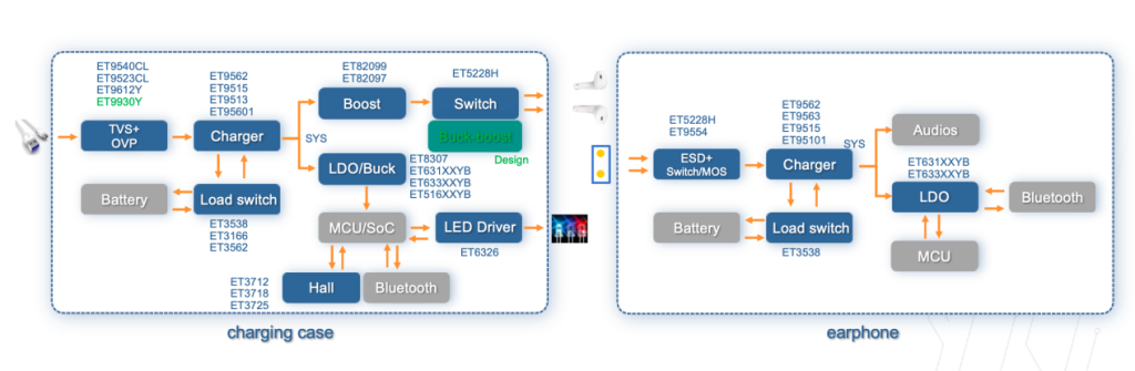
True Wireless Stereo Application
Why the Hall Switch Circuit Has Become a Power-Critical Component
In a typical TWS application, the hall switch circuit is used to detect magnetic state changes caused by the opening and closing of the charging case, the position of earbuds, or accessory covers. Unlike intermittent sensors, the hall switch circuit usually resides in the Always-On domain, operating 24/7 even when the main SoC is in deep sleep.
Historically, many hall switch circuits were designed to operate at 1.8V or 3.3V. While this approach was acceptable in earlier architectures, it introduces clear disadvantages in modern ultra-low-power systems. Supplying a higher-voltage hall switch circuit from a 1.2V-based platform requires additional LDOs, which increase static power loss, add quiescent current, and complicate the power tree. Over time, these inefficiencies accumulate and directly reduce standby performance.
As a result, hall switch circuit selection is now closely tied to voltage domain planning and Always-On power budgeting.
The Industry Shift Toward 1.2V Hall Switch Circuits
Driven by advanced semiconductor processes and aggressive battery life targets, leading TWS SoC platforms have standardized on 1.2V for both the core voltage and the Always-On domain. This shift reflects a broader system-level optimization strategy rather than a single-device improvement.
From an architectural perspective, the most efficient hall switch circuit is one that can be directly powered by the 1.2V Always-On rail. A native 1.2V hall switch circuit eliminates voltage conversion stages, reduces leakage paths, and simplifies system design. More importantly, it allows engineers to scale Always-On functionality without disproportionately increasing standby power consumption.
In this context, 1.2V operation is no longer a niche requirement—it is becoming the baseline for next-generation TWS designs.
ETEK’s 1.2V Hall Switch Circuit Solutions
Recognizing this trend, ETEK has developed a dedicated portfolio of hall switch circuit solutions optimized for 1.2V Always-On systems. These devices are designed not only to meet voltage requirements, but also to address the real-world constraints of TWS products, including size, reliability, and long-term stability.
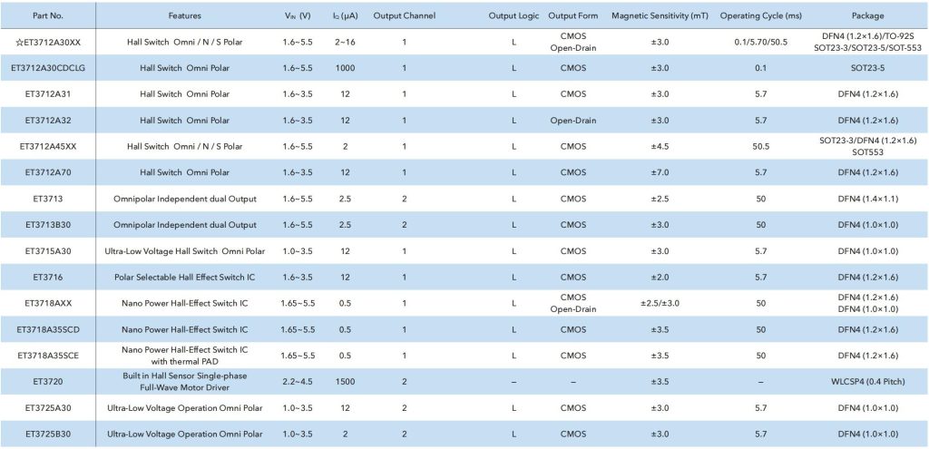
The ET3725Axx series is a dual-output, omnipolar hall switch circuit that supports a wide operating voltage range from 1.0V to 3.5V, making it naturally compatible with 1.2V SoC platforms. Its omnipolar sensing capability allows flexible magnet placement, which simplifies mechanical design in compact charging cases. With an ultra-small 1mm × 1mm DFN4 package, this hall switch circuit fits easily into highly integrated PCBs where every fraction of a millimeter matters.
For applications with simpler detection requirements or stronger cost sensitivity, ETEK also offers the ET3715A series, a single-output hall switch circuit that likewise supports 1.2V operation. This provides designers with greater flexibility when balancing functionality, cost, and power consumption, without compromising compatibility with low-voltage Always-On domains.
ETEK Hall Switch Circuit
Proven Performance in High-Volume TWS Projects
Specification alignment alone is not sufficient for consumer electronics. Reliability under continuous operation is equally critical for any hall switch circuit used in TWS systems. ETEK’s 1.2V hall switch circuit family has already been adopted in Samsung’s flagship TWS projects, with cumulative shipments exceeding one million units.
This large-scale deployment demonstrates stable magnetic switching behavior, consistent sensitivity across temperature variations, and reliable operation under long-term Always-On conditions. For OEMs and ODMs, such mass-production validation significantly reduces design-in risk and accelerates time to market.
System-Level Advantages of Native 1.2V Hall Switch Circuits
By selecting a hall switch circuit that directly supports 1.2V operation, designers gain multiple system-level benefits:
✔Lower standby power consumption due to reduced quiescent current and fewer LDO stages
✔A simplified power architecture with fewer external components
✔Reduced PCB area and BOM cost
✔Better scalability as Always-On features continue to expand
As TWS products evolve toward more intelligent, context-aware interaction, these advantages become increasingly important.
Conclusion: Hall Switch Circuit Design for the 1.2V Era
As TWS SoC platforms firmly enter the 1.2V era, Always-On components must evolve accordingly. The hall switch circuit, as a continuously powered sensing element, plays a decisive role in defining overall system efficiency.
ETEK’s 1.2V hall switch circuit portfolio is designed to meet these new requirements, combining ultra-low-voltage operation, compact packaging, and proven reliability in high-volume consumer applications. For engineers building the next generation of TWS and portable electronics, choosing the right hall switch circuit is a foundational step toward achieving longer battery life and a cleaner system architecture.
For samples, technical support, or design-in inquiries:


