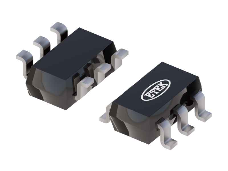
ET74LVC1G175
 Contact
General Description
The ET74LVC1G175 is a low-power, low-voltage single positive edge triggered D-type flip-flop with individual data (D) input, clock (CP) input, master reset (MR) input, and Q output. The master reset (MR) is an asynchronous active LOW input and operates independently of the clock input. Information on the data input is transferred to the Q output on the LOW-to-HIGH transition of the clock pulse. The D input must be stable one set-up time prior to the LOW-to-HIGH clock transition for predictable operation. The inputs can be driven from either 3.3V or 5V devices. This feature allows the use of this device in a mixed 3.3V and 5V environment. This device is fully specified for partial power-down applications using IOFF. The IOFF circuitry disables the output, preventing the damaging back-flow current through the device when it is powered down. Schmitt trigger action at all inputs makes the circuit highly tolerant of slower input rise and fall times.
Features
- Wide Supply Voltage Range from 1.65V to 5.5V
- 5V Tolerant Inputs for Interfacing with 5V Logic
- High Noise Immunity
- ±24mA Output Drive (VCC = 3.0V)
- CMOS Low Power Consumption
- IOFF Circuitry Provides Partial Power-down Mode Operation
- Direct Interface with TTL Levels
- Inputs Accept Voltages up to 5V
- Multiple Package Options
- Latch-up Performance Exceeds 200mA per JESD78, Class II
Technical Documentation
| Type | Title | Format | Date |
|---|---|---|---|
| Datasheet | ET74LVC1G175 Datasheet | 2025-12-07 |

 EN
EN


 Specification
 Sample


